Cortex Family


Home Page
STM32 Page


INDEX


Introduction
Architecture
Parts Cost
The Cortex Mx core, instructions and compatibility
Performances & differences from M0, M1, M3 and M4 core
Energy Efficiency
Why use CORTEX M family instead of 8 and 16 bit MCU
CMSIS
Link
Glossary


Introduction


ARM is a 32-bit reduced instruction set computer (RISC) instruction set architecture (ISA) developed by ARM Holdings.
It was named the Advanced RISC Machine, and before that, the Acorn RISC Machine.
The ARM architecture is the most widely used 32-bit instruction set architecture in numbers produced.
Originally conceived by Acorn Computers for use in its personal computers, the first ARM-based products were the Acorn Archimedes range introduced in 1987.
The relative simplicity of ARM processors makes them suitable for low power applications. As a result, they have become dominant in the mobile and embedded electronics market, as relatively low-cost, small microprocessors and microcontrollers.
In 2005, about 98% of the more than one billion mobile phones sold each year used at least one ARM processor.
As of 2009, ARM processors account for approximately 90% of all embedded 32-bit RISC processors and are used extensively in consumer electronics, including personal digital assistants (PDAs), tablets, mobile phones, digital media and music players, hand-held game consoles, calculators and computer peripherals such as hard drives and routers.
(source: Wikipedia)
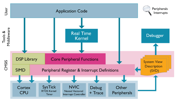
For those unfamiliar with the family CORTEX we give some preliminary clarifications.
In general, the main features of ARM core are:
Core 32bit
RISC architecture
Excellent relations DMips/Watt
Some years ago, ARM has launched a new generation of its core identified by the name: CORTEX
The family is divided into three subfamilies:
The x indicates that after the letter (A, R, M) is a number that identifies in detail the core.

The ARM families are divided in three macro areas, see below.


In this page we will highlight the Cortex Mx family (Embedded Processors), in particular we will analyze the M0, M3 and M4.
Embedded Processors are primarily focused on delivering highly deterministic real-time behaviour in  a wide range of power sensitive applications.  These processors often execute a Real-Time Operating System (RTOS) alongside user-developed application code, and hence only require a Memory Protection Unit (MPU) as opposed to the MMU available in the Application Processors.
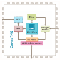
The Cortex™-M0...M3 processors have been designed to deliver  industry-leading deterministic behaviour, lowest sleep and dynamic power, and smallest area possible whilst maintaining high processing efficiency.
The Cortex-Rx delivers a roadmap from Classic ARM processors including the ARM7...11™ families, enabling existing applications to be easily ported to a higher performance platform.
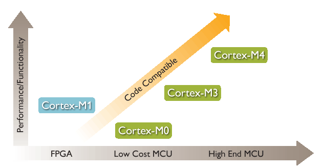
The family CORTEX Mx is divided into four subgroups that are: M0, M1, M3 and M4.
The computing power of CORTEX Mx is in the range from 0.84 DMips/MHz to 1.25 DMips/MHz.
ARM consider obsolete the families: ARM7, ARM9 and ARM11.
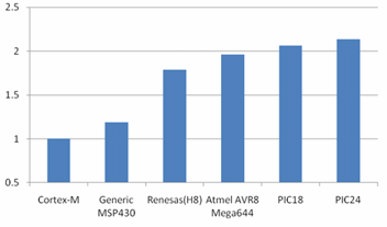


Architecture


The ARM architecture supports implementations across a wide range of performance points.
It is established as the leading architecture in many market segments. The architectural simplicity of ARM processors leads to very small implementations, and small implementations mean devices can have very low power consumption. Implementation size, performance, and very low power consumption are key attributes of the ARM architecture.


ARMv6M architecture is designed for low-cost, high-performance devices providing a 32-bit powerful solution in a marketplace previously dominated by 8-bit devices.  Its 16-bit Thumb instruction set architecture allows designers to create cost-effective devices with minimal gate count.  The consistent interrupt handling structure and programmer's model provides a full upwards-compatible path for all Cortex-M series processors from the Cortex-M0 to the Cortex-M3 processor.
ARMv7 architecture profiles implement Thumb-2 technology which is an optimized, mixed 16/32-bit instruction set providing the performance advantages of the 32-bit ARM ISA with the code size advantages of the16-bit Thumb ISA, while retaining complete code compatibility with existing ARM solutions.


UP


Parts Cost


It is no secret that ARM Cortex M family are pushing the price/performance ratio to heretofore unseen levels.
The main target of comparison between ARM Cortex M family is traditional 8 and 16 bit microcontrollers.
Long considered the cheapest mainstream alternative, 8 bit microcontrollers are facing considerable competitive pressure from ARM Cortex M family.
In general, when the pin-out of the 8/16 bit MCUs are close to 28/32, it should be evaluated also at the CORTEX M family.
STM and NXP Cortex M3 price is under 1$ for 10Kps.


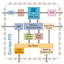
The Cortex Mx core, instructions & Compatibility


Below there are the M0, M3 and M4 core.
   

Below there is the instruction set concerning M0, M1, M3, M4 and M4F.
As you see there are a complete binary compatibility.


Performances & differences from M0, M1, M3 and M4 core


Performance


Code size


Differences from M0, M3 and M4


UP


Energy Efficiency


Today there is a particularly strong energy problem for which all equipments should consume as little as possible.
Cortex M series run at lower MHz or with shorter activity periods:
Architected support for sleep modes
Work smarter, sleep longer than 8/16-bit


UP


CMSIS 


CMSIS means: Cortex Microcontroller Software Interface Standard

The ARMŽ Cortex™ Microcontroller Software Interface Standard (CMSIS) is a vendor-independent hardware abstraction layer for the Cortex-M processor series
The CMSIS enables consistent and simple software interfaces to the processor and the peripherals, simplifying software re-use, reducing the learning curve for new microcontroller developers and reducing the time to market for new devices.

Creation of software is acknowledged as a major cost factor by the embedded industry.
By standardizing the software interfaces across all Cortex-M silicon vendor products, this cost is significantly reduced, especially when creating new projects or migrating existing software to a new device.


The CMSIS consists of the following components:

  • Peripheral Register and Interrupt Definitions: a consistent interface for device registers and interrupts
  • Core Peripheral Functions: access functions for specific processor features and core peripherals
  • DSP Library: optimized signal processing algorithms and for Cortex-M4 support of SIMD instructions
  • System View Description (SVD): XML file that describes the device peripherals and interrupts. 
The standard is fully scalable to ensure that it is suitable for all Cortex-M processor series microcontrollers from the smallest 8 KB device up to devices with sophisticated communication peripherals such as Ethernet or USB. 
(The memory requirement for the Core Peripheral Functions is less than 1 KB code, less than 10 Bytes RAM).


The CMSIS has been developed in close partnership with several key silicon and software vendors. This collaboration, together with feedback from previous solutions, has resulted in an easy-to-use and easy-to-learn programming interface for Cortex processor-based devices. Current CMSIS Partners include (Jan-2012):


(source: ARM)

UP


LINK

Documentation for Cortex-M device users

Software development tools for Cortex-M device users

Find Cortex-M based microcontrollers


Cortex-M Series Processor Documentation


UP


UP


Home Page
STM32 Page